In this post I’ll describe the CPU board in more detail, what are its components, how it interacts with other modules and what decisions I took while making it.
This serves as a continuation to my previous post about the video game console I’ve designed and made.
This post is a bit more technical, maybe too much for some and maybe not enough for others.
I do hope it’s useful for someone, that’s the intention making these posts.
Decisions
The heart of the CPU board is, of course, the CPU itself.
For this console I had to get a CPU worthy of a “retro” styled video game console, also I wanted a “real” discrete CPU, I didn’t a modern architecute, no multi-core and I didn’t want to emulate a CPU in a microcontroller, for example.
So with these goals in mind I started looking for an interesting CPU (that wasn’t too hard to mess with).
CPU: 6502 vs Z80
I quickly came to two alternatives, two 8-bit CPUs, the Z80 and 6502, they are both iconic and are still being manufactured today.
The 6502 (sometimes as a variant) was used in such machines as:
- Apple I
- Apple II
- Nintendo Entertainment System
- Commodore PET
- Commodore VIC-20
- Commodore 64
- Atari 2600
- Atari 5200
- Atari 7800
- many more…
It was a relatively cheap CPU at the time and so it was used in many commercial products.
Nowadays the variant WDC 65C02 is available in many electronic component stores and can be run at up to 14Mhz which is an extremely higher frequency than its older models.
The Z80 was/is used in the following machines:
- Sinclair ZX Spectrum
- Nintendo Gameboy
- MSX
- Sega Master System
- TRS-80
- Texas Instruments TI-83 Calculator
- Also many more…
This CPU can also be found today in multiple electronic component stores in models that operate at 6, 8, 10 or 20 Mhz.
The Z80 is usually clocked at a higher frequency than a 6502 is, but it is “slower” to execute similar instructions. Each instruction will take more clocks than a 6502, even though, in my opinion, it is not that simple to compare both CPUs, I would say a 4 Mhz Z80 is more or less equivalent to a 1 Mhz 6502 in terms of performance of equivalent instructions.
One of the reasons the comparison of performance is not that easy is because the Z80 has some 16-bit instructions and more registers available.
The Z80 has the A, H, L, D, E, B and C registers that can be used for multi-purposes. They can also be grouped for 16-bit operations, HL, BC, DE.
And the feature I found the most interesting in the Z80 CPU was the fact that along with a 16-bit memory space, it also has a 16-bit IO space (reading the Z80 CPU manual one might think that the IO space is only 8-bit, but it’s actually 16-bit on all Z80s).
By having this, I could have the entire memory space for code and data while reserving the IO space to access the external components (for graphics, sound and IO).
So I ended going with the Z80 for my video game console and one clocked at 10 Mhz, because it seemed powerful enough for what I wanted.
Adding other components
Connecting to RAM and ROM
After choosing the CPU, because I needed the Z80 to access some software as soon as it started running after being turned on, I decided to connect it to an EEPROM which is a ROM chip I can reprogram with code and data, the idea was for this chip to hold the bootloader software, a software which reads the programs available in the SD Card and then loads the selected program to RAM.
Even though reprogramming the EEPROM is not the most practical thing, the bootloader wouldn’t need to be updated very often so it was fine for it to be stored this way.
Other consoles have software stored in a ROM in the console, such as the Sega Master System, if you turn on this console without any game in it you will be greeted with a screen with information and there’s even a hidden playable game, most other consoles of that era without a cartridge inserted just show a black screen at most.
So in order for the ROM to be acessible when the Z80 is initially activated, it must be accessible on address 0 (or 0000h in hexadecimal) because it’s on this address that the Z80 starts executing code wants it’s switched on.
I decided on an 8 KB ROM as it was enough to store a sizable bootloader program.
After the ROM, the console needed RAM, of course, data has to be stored and retrieved from somewhere and since the Z80 can access 64 Kb of memory at once, the RAM would fill the rest of accessible memory space, 56 KB.
Some might be wondering if 56 KB of RAM is “too much”, consoles, especially the ones from the 3rd generation, had similar CPUs but not nearly this much RAM:
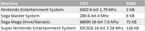
The reasons to go for this amount of RAM are, well, first of all RAM is not as expensive as it once was, so I wanted to fill all the available memory space with RAM, and also this console has a difference from 3rd generation consoles, the games/programs are in an SD Card and in order for them to be executed by the CPU they need to be loaded into memory first.
So the RAM is not only for data like the consoles above (they could also be used for code in some rare situations) but also for code, inside the cartridges of 3rd and 4th generation consoles there were ROMs with the code and data (graphics, sound, etc), this console doesn’t have that, accessing the SD Card is too slow to be done the same way ROM or RAM is accessed, so code cannot be run directly from it.
Other consoles that didn’t have the games in cartrdiges had similar approaches, such as the Mega-CD or the Atari Jaguar, for example, these had to load the code and data from a CD into RAM, before executing the program and of course all later consoles did this when cartridges were abandoned all together.
Switching between ROM and RAM
This may be basic stuff for most of you reading this, but it could help those who are trying to figure out how a CPU can access different chips simultaneously, something I had to go through as well.
Because ROM and RAM are in the same address and data buses, in order for the CPU to access the 8 KB ROM and 56 KB RAM, it needs to activate the ROM and deactivate the RAM when the Z80 accesses memory positions from 0000h to 1FFFh (8191 in hexadecimal or 8K - 1), and do the opposite when the Z80 accesses memory positions from 2000h (8192 or 8K) to FFFFh (65535 or 64K - 1).
Each ROM and RAM chip has a CE pin which means “Chip Enable”, when this pin receives a low signal the chip becomes active, and when it receives a high signal it becomes inactive. So all we need to do is send a low signal to ROM and high to RAM and vice-versa depending on which address the CPU is trying to access.
Let’s have a look at the pinout of a typical Z80 CPU:
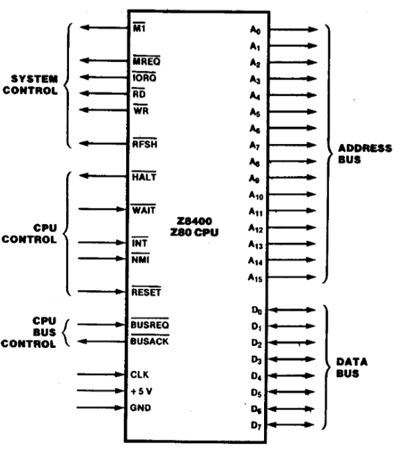
Whenever the Z80 makes a memory request it sends a low signal through the MR pin (or MREQ as shown above) and sets the address pins to the destination address (pins A0 to A15). And if it’s a read, it expects data to be sent to its data pins, and if it’s a write then it sends data through these same pins. The exact timings for these things can be found in the CPU’s manual.
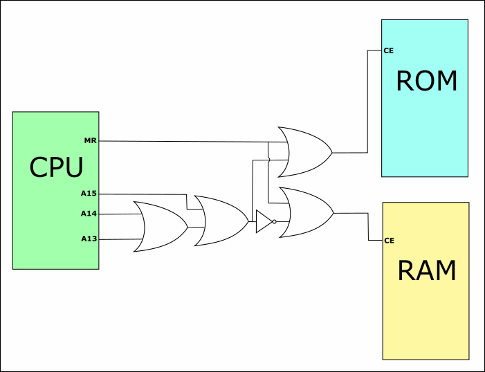
To afect the CE pins of our ROM and RAM we can use these signals above:
- CE ROM = MR or A15 or A14 or A13
- CE RAM = MR or not (A15 or A14 or A13)
Here is a diagram of the connections described above for those who like diagrams:
With the proper connections, in Z80 code, when I access the lower 8 KBs I will access ROM (there’s no use in trying to write to it, because it’s read-only):
; Reading from address 0x0100, that's reading from the ROM
ld a, $0100
And when I access an address higher than or equal to 8 KB I will access RAM:
ld a, ($3400)
inc a
ld ($3400), a
As you may have noticed the lower 8 KB of RAM will never be accessed. This is a bit of a waste, but I wasn’t too much concerned about that.
Connecting to IO, PPU and SPU
In order for the CPU to access the other modules (IO, graphics and sound) I needed to interface it in a similar way as it was done for the ROM and ROM.
The big difference was that because the whole memory space was occupied by the ROM and RAM, I wanted these to be accessible through the IO space of the Z80 CPU.
For the graphics (PPU) and sound (SPU) I am using dual-port SRAMs as an interface between the CPU and these systems. For the IO MCU the CPU interfaces with a microcontroller, but it actually acts an SRAM, in terms of protocol, just much slower.
For the IO MCU I needed 256 bytes of address space (actually not that much but I reserved this much space anyway), for the graphics (PPU) I needed 4 KB and for the sound (SPU) I needed 2 KB.
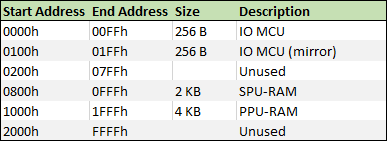
I have 64KB of IO space available and that’s plenty, so this is how I mapped them:
When accessing the IO space (using the IN and OUT instructions of the Z80), the CPU, instead of the MR pint, will set the IO pin low (or IORQ as in the picture above).
And from the table above, we know that for the IO MCU we only use the lower 8 bits of the address lines and 8 higher ones have to be all low (actually I only checked 7 due to a limitation I’ll explain below and that’s why there’s a mirror and from 0x0000 to 0x00FF is the same as from 0x0100 to 0x01FF).
For the PPU, we’ll want to access it when the 4 upper address lines are 0001 and the SPU when the upper address lines are 00001.
One thing about the PPU RAM, is that I needed 4 KB, but could only find chips with up to 2 KB of dual-port SRAM, so I had to use two chips instead of one and therefore had to divise the logic to connect to both PPU RAM 1 and PPU RAM 2.
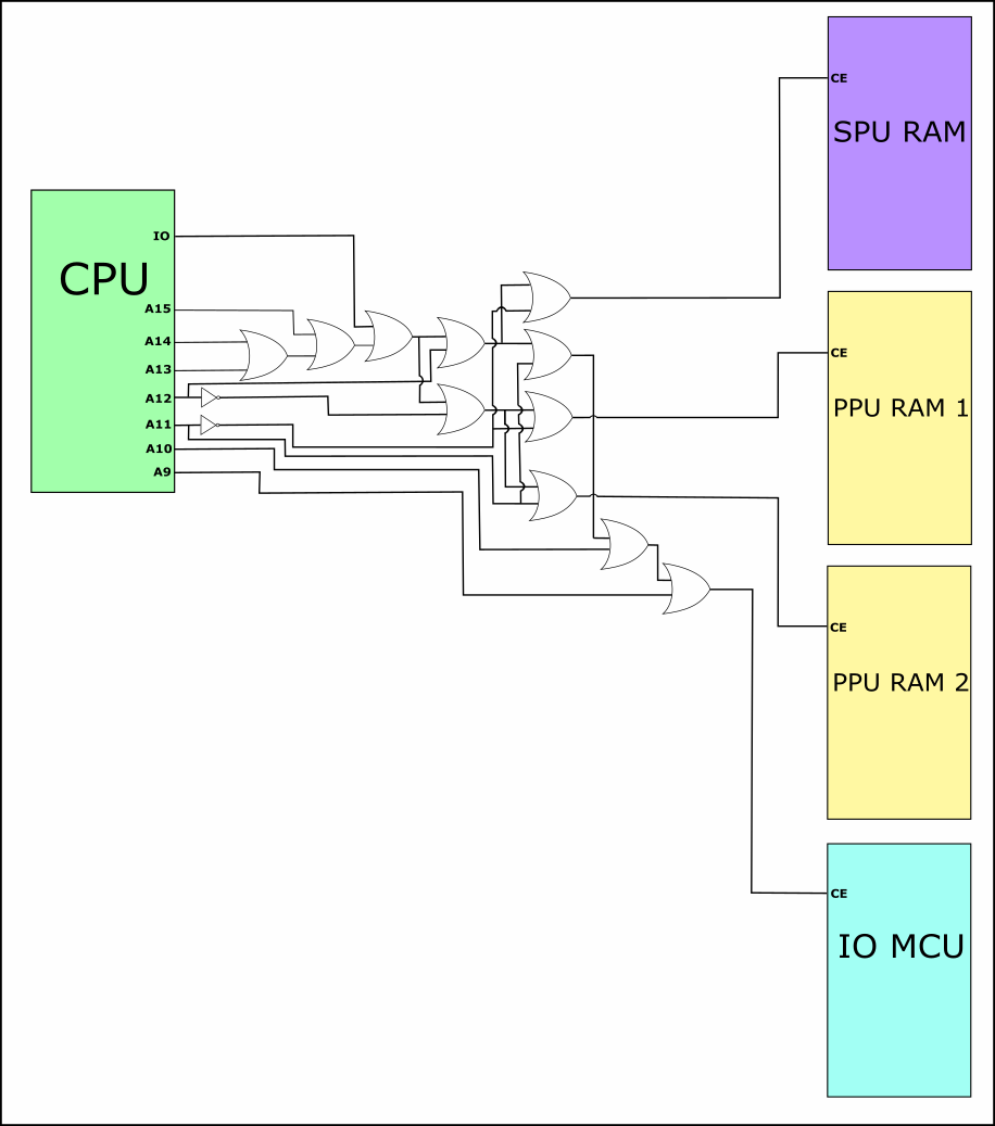
So the corresponding CE signals for the IO MCU, PPU RAM and SPU RAM are the following:
- CE IO MCU = IO or A15 or A14 or A13 or A12 or A11 or A10 or A9
- CE PPU RAM = IO or A15 or A14 or A13 or (not A12)
- CE PPU RAM 1 = IO or A15 or A14 or A13 or (not A12) or A11
- CE PPU RAM 2 = IO or A15 or A14 or A13 or (not A12) or (not A11)
- CE SPU RAM = IO or A15 or A14 or A13 or A12 or (not A11)
Here is another diagram describing the connections above (I just realised that this picture is most likely not particularly helpful, but it took me a long time to make, so here it is):
In Z80 code, acessing the IO MCU, can be done as such:
; Reading from the IO MCU at position 0x00 which is reading from the RS232 interface
ld bc, $0000
in a, (c)

; Writing to the IO MCU at position 0x01 which is writing to the RS232 interface
ld bc, $0001
ld a, 33
out (c), a
Accessing the PPU:
; Reading from the PPU RAM at address 0x001 that for the CPU is address 0x1001
ld bc, $1001
in a, (c)

inc a

; Writing the incremented value to the same address
out (c), a
Accessing the SPU:
; Reading from the SPU RAM at address 0x000 that for the CPU is address 0x0800
ld bc, $800
in a, (c)

; Writing to the FM Control byte of the SPU (address 0x0001) that is 0x0801 for the CPU
lb bc, $801
ld a, 1
out (c), a
There is another connection to the CPU, one connecting this component to the PPU, which is the NMI signal.
Whenever the PPU is about to start drawing a new frame, it copies the contents of the PPU-RAM to an internal RAM and then it signals the CPU throught the NMI signaling that a new frame is starting and new information ca be written to the PPU-RAM.
The signal to the NMI pin is set to low momentarily which causes a non-maskable interrupt (NMI) to trigger in the Z80 and the code jumps to position 66h.
This is important for programs that have code that executes every frame, such as getting the players controller status, updating the graphics, sound, etc.
Putting it all together
In terms of components, I needed of course a Z80 CPU in a DIP package and that could run at 10 Mhz because why not.
For the ROM I picked up an 8KB EEPROM, which, like I mentioned above, is not as practical as having code in media such as an SD card, however it is a rewritable ROM so it enables me to rewrite it whenever I need to update the bootloader.
For the RAM I used an 128 KB SRAM, I’m not using all of it, but I couldn’t really find a 64 KB RAM chip, only 32 KB or 128 KB, so I’m using a 128 KB RAM instead of two 32 KB RAM ICs.
Now for the glue logic, that is, for the logic in connecting the CPU to the other components (the one described above with all the diagrams), originally I used quite a few 74 series ICs for the ORs and NOTs needed. However I found that I could use a PLD (Programmable Logic Device) which allows me to program the logic between input and output pins and this way a single PLD chip replaces quite a few 74 series chips. One limitation of the PLD I chose is its pins, there weren’t enough to map all the address lines and that’s why the connection between the CPU and the IO MCU was mirrored as shown above, still this wasn’t a deal-breaker.
Also fortunately I was able to find an affordable programmer for the EEPROM and the PLD. ROM programmers can be very expensive.
I also placed the PPU-RAM in the CPU module, simply because the video module is huge and the CPU module was quite small, so, as I needed 4 KB of RAM for the SPU-RAM, I went for two 2 KB Dual-port SRAM ICs. Dual-port SRAM is a chip that can be simultaneously connected to two different components with separate buses, this is much easier than having two components alternate to access the same single-port SRAM chip, the dual-port SRAM ICs are, however much more expensive, not as fast and take up a lot of space, so they come in small sizes in terms of memory especially when in DIP package. Good thing 4 KB is all I needed for the interface between the CPU and the PPU.
The board is then composed of:
- Z80 CPU - Z84C0010
- 128KB SRAM 55ns - AS6C1008
- 8KB EEPROM 120ns - AT28C64
- PLD - ATF16V8B
- 2 x Dual-port 2KB SRAM 100ns - IDT7132
How fast is it
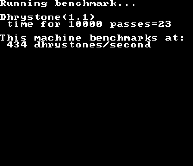
I have measured the computational power using a ported version of the Dhrystone benchmark, I got a version from 1986 (version 1.1) which was used to measure the processing power of systems back then.
Here is the screenshot of the result when running on my console (it’s actually a screenshot of the emulator running the benchmark, but the result is the same):
This result of course depends not only in the CPU and the frequency at which is running, but also in how the code itself is compiled and the performance of the auxiliar code, such as multiplication and division as well as operations involving numbers of greater size (the Z80 CPU doesn’t have a multiplication nor a division instruction, they must be done by software using additions and subtractions).
The benchmark software was compiled using SDCC version 3.8.0.
In order to give some context to the result of the benchmark, here is a table with the benchmark’s result in other systems:
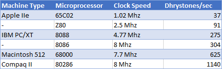
So the result is what we could expect of a machine with a Z80 CPU running at 10 Mhz, no surprise here.
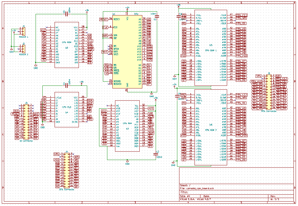
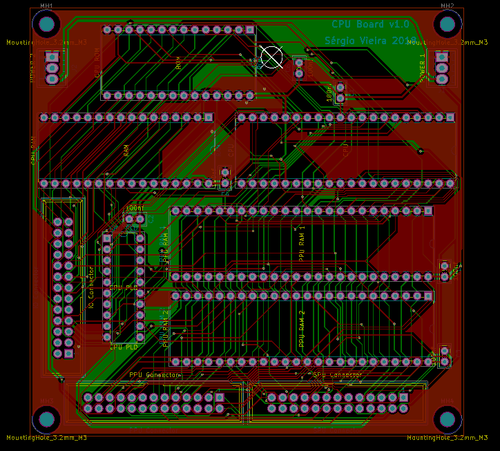
Designing the PCB
This was the first board I’ve ever designed a PCB for.
Using Kicad, I first designed the schematics:
Then the PCB:
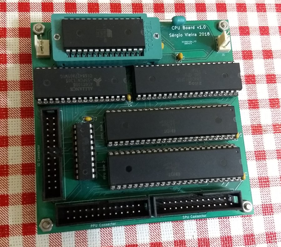
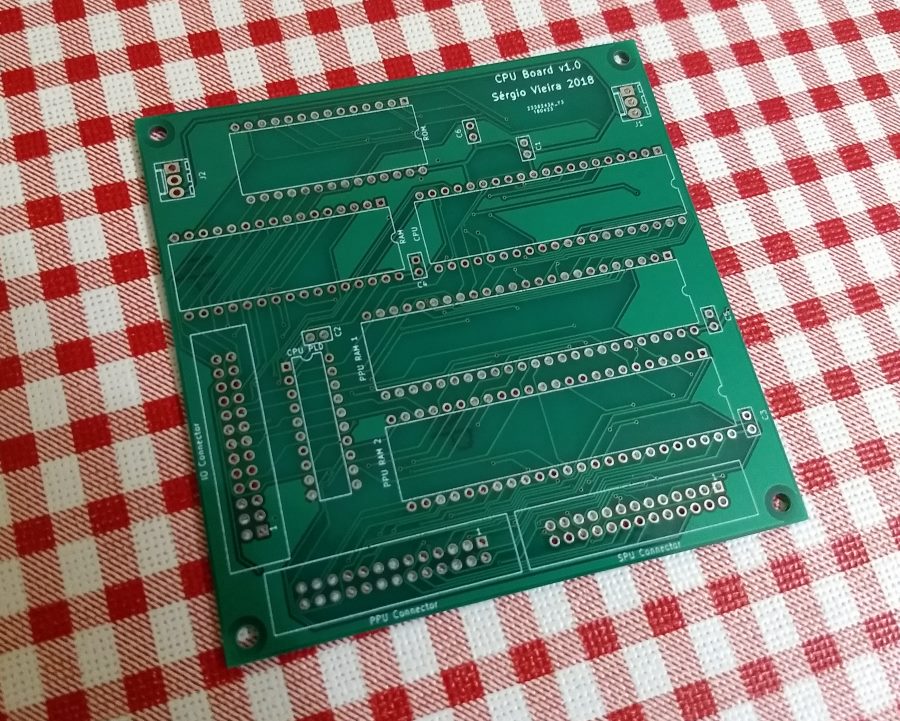
This is the final product:
And here after being populated:
The components seem very close to each other, this is because it was cheaper to order smaller PCBs, so I tried to make it small enough as not pay more then I had to.
I did use an auto-router to layout most of the connections between the components. And very likely electronic engineers reading this will probably find many flaws in the design.
However and even though I’m no expert at designing PCBs (much like at anythhing else), I think it turned out ok and it works, which is the most important thing. Of course any criticism or advice is welcome, I’m always looking to improve myself.
And this is it
I hope this helps someone with his or her projects, thank you for reading it.
I’m thinking of writing other posts about Video, Sound and other projects I have (hopefully I don’t take as long).
As always, any question or suggestion please comment below or reach me in my twitter account @IntRegister