This is yet one more post about the retro homebrew console I’ve made and sumarized in this post.
This time I’ll talk about the video board, the most complex part of the project.
It’s by no means flawless and it took me the most amount of time to perfect and make it work.
This post like the last one is heavier on the technical side, I will try to explain “simpler” concepts along with more complex ones for those who read this and are not exactly familiar with all the technical knowledge necessary to design and build a project like this.
And on a technical note, in this post you will see AVR assembly code, this is the code used in programming AVR microcontrollers, they work with 5V VCC and can run at 20Mhz and have a performance of almost 20 MIPS, so they were good for this project.
In this system I’ve used two of these microcontrollers, an Atmega324 and an Atmega1284, they’re both similar in that they have 32 GPIOs (general-purpose input-outputs) divided into 4 ports (Ports A, B, C and D), each with 8 GPIOs.
This information is useful when trying to understand how I’ve used them.
Initial goals
The goal for the console’s video system, was for it to be powerful enough to support a platforming game (like old Mario games).
This basically means at least one scrollable background layer and sprites.
I also didn’t want to use any off the shelf component that would provide me with this (not that there are many out there).
The goal was to design something from scratch, I believe that graphics are in many ways what define a retro console. A lot of times on older consoles, one could identify on which console a game is being played just by the way it looked.
So I decided to build something somewhat unique myself.
Another goal I had was for the video system’s output to be an analog TV signal, preferably a composite signal.
About the type of composite signal, back in the day, video game consoles came in various versions, some outputing PAL, others NTSC (used in the USA and Japan, for example) and others some more obscure video signals.
Since I’m from Portugal, a PAL video signal, because it’s the standard here (or at least it was before digital TV) and in most of Europe.
Learning from existing retro consoles
Looking at how 3rd and 4th generation video game consoles worked, I’ve learned that the CPU would not send information to draw individual pixel or even polygons like with nowadays’ GPUs.
Instead each scene was composed of fixed elements and the CPU would set the attributes of the scene to be rendered by writing information to the video system’s registers and/or RAM.
Let’s take a look at a scene from an NES game. Its components are:
- A background layer
- up to 64 sprites (only 8 visible per line at one time)
It’s not as versatile as today’s system in terms of defining what the player sees, however, despite the limitations and also with some clever tricks (like changing the scene’s definition mid-frame, for example), it’s possible to make some great games.
This technique has the advantage, of course, of not needing the CPU to do any of the heavy lifting when it comes to graphics, it doesn’t need to define where each pixel will be drawn nor every detail of the scene.
For every frame, the CPU only needs to update certain properties of certain components, like the sprites’ positions and attributes, background scroll position, etc.
Challenges of building a Video System
I had already figured that I was going to use an SRAM (dual-port) chip to store the scene’s definition and serve as a place for the CPU to set these definitions and the PPU to read from them to know what so as to know what to render (I called it PPU-RAM, giving components names helps, even if they’re kind of silly, trust me).
So now in order to build my own video system I just needed to find out what I was going to use to read the scenes’ definition and render it to the TV screen.
All of the consoles of the 80s and 90s had ASICs for video, chips designed especially for this purporse, so rendering was done by specialised hardware.
Obviously that wasn’t an option for me, the closest thing to it and the most obvious choice (not at the time I started this project, though) was using an FPGA.
However, just like with many other things, when I started this endeavour I had very little knowledge of electronics, so dealing with FPGAs was not an option either.
The option left were microcontrollers, I had become quite experienced with AVR microcontrollers and knew that they were at least powerful enough to generate a viable video signal.
I had seen something like this before in Uzebox, an awesome video game console project based on a single overclocked AVR microcontroller and it was a great inspiration for my own projects.
So I decided to use these AVR microcontrollers as the basis for my console’s video system.
Math
Using a 20 Mhz AVR microcontroller and a PAL video signal (which uses a screen refresh frequency of 50 Hz) meant I had 400.000 clocks to render a frame and also generate the adequate TV signal with the correct timings.
An added complexity is the fact that I have to interact with external memory, this is gonna be costlier in terms of performance than using the microcontroller’s internal RAM.
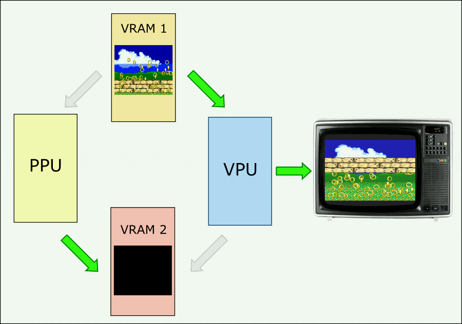
One of the first decisions was to break the system into two separate microcontrollers, one to render frames, the PPU (Picture processing unit) and one to generate the video signal according to the frame drawn, the VPU (Video processing unit).
This also meant that I was going to have to find a way to interface the two of them, the PPU and the VPU.
I did this using a double-buffering solution, adding 2 RAM components (VRAM 1 and VRAM 2).
These components would each store a rendered frame.
The idea was to let the VPU exclusively generate the video signal getting the frame information from one of the VRAMs while the PPU was exclusively dedicated to rendering a frame and dumping it on the other VRAM and then they would switch VRAMs and repeat.
The VPU decides when the switch of VRAMs occurs and sends a signal to the PPU to start rendering another frame.
Having one of the microcontrollers dedicated to render the frame scene, means the 400.000 clocks are dedicated to producing an image and storing it in VRAM (20 Mhz for 1/50 seconds means 400.000 clocks).
This means that for a resolution of 256x240 pixels, for example, (the same as the NES), we have 61.440 pixels, so we would have about 6.5 clocks per pixel on average.
This means that the firmware used to generate a frame would only have 6.5 clocks available on average for each pixels rendered.
Because when the AVR architecture, most instructions take only one clock (in comparison, Z80 architecture takes at least 4 clocks and can go up to 19 or more), means that I have about 6 and half instructions per pixel.
This is ok, but not great, at least for the amount of graphical complexity I was aiming for and after a few tests I reached the conclusion that just to draw a background and some sprites I would need more than that.
So I made a couple more compromises:
-
Reduce the framerate from 50 fps to 25 fps (I didn’t really want this as I would very much prefer the full 50 fps, but I had to do it)
-
Settle for a frame resolution of 224x192 pixels (43.008 pixels in total)
With these changes I now had 800.000 clocks to draw 43.008 pixels, which means about 18.6 instructions per pixel, giving me some leeway to get some nice graphical features to the video game console.
Another thing I wanted to add, was a RAM to store custom graphics.
This CHR-RAM would store 128 KB of graphical data, divided into 8x8 pixel characters (just like other retro consoles).
However having this RAM meant that I needed for the CPU to somehow store data in it, and for the PPU to access it to use its information to render the scene.
This added yet more complexity and had to be taken into account when estimating the clocks needed to render, however it was something I really felt was necessary.
I could have some pre-defined graphics inside the PPU and have another mode to draw using the CHR-RAM graphics.
Below I describe how I’ve optimized the access to this memory.
The full capabilities for the video system weren’t decided right way, I just tried to cram as many features as I could in those 800.000 clocks to render a frame.
One bad thing that came out of these decisions, mainly the double-buffering and the 25 fps was the latency.
This is a drawback and at times I felt it was going to be a show-stopper.
The latency between user input to the frame being shown on a TV is between 100 and 120 milliseconds.
This is a lot, however using it, I feel it’s manageable even in action games (using a CRT TV possibly helps).
Implementation details
So, so far I knew I had two components, the VPU and the PPU.
Since the VPU is the component that is on strict timing constraints, as it needs to send information to the TV in a steady stream, it has to be the one controlling when the PPU is going to draw a new frame.
So these two need to be connected by a signal that changes whenever the VPU switches which VRAM each one is connected to.
They are also both connected to both VRAMs in order to perform the aformentioned double-buffering.
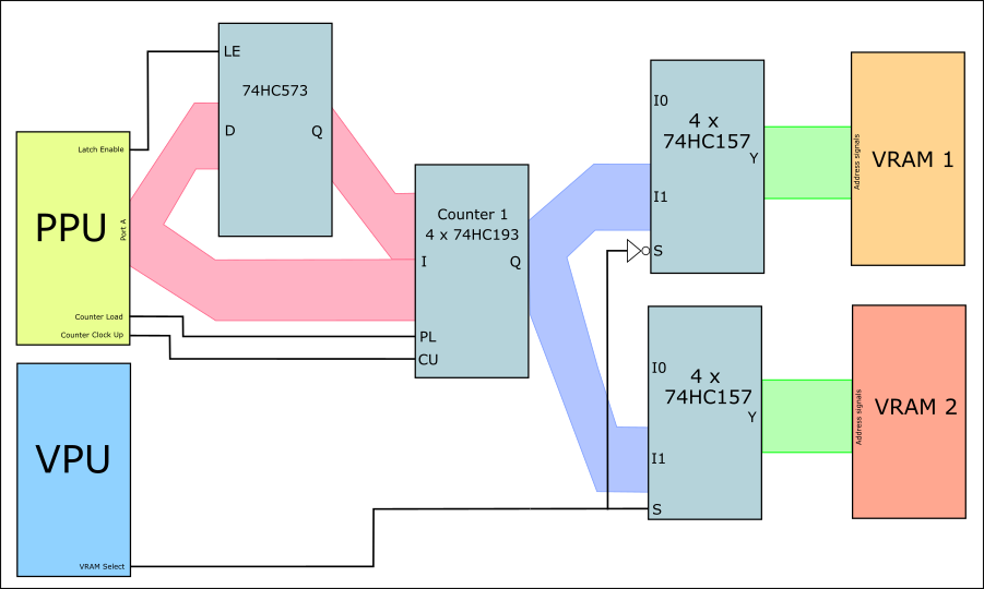
Because VRAM is not dual-port RAM and just 2 normal SRAM modules (I couldn’t find dual-port RAMS with such a big capacity), I needed to find a way to connect the two components to both VRAMs where both VPU and PPU could work simultaneously in different VRAMs.
The problem of connecting two components to the same SRAM chip is that they both share the same address and data bus as well as control signals. This means that while one is accessing the SRAM the other one needs to not output any signals whatsoever.
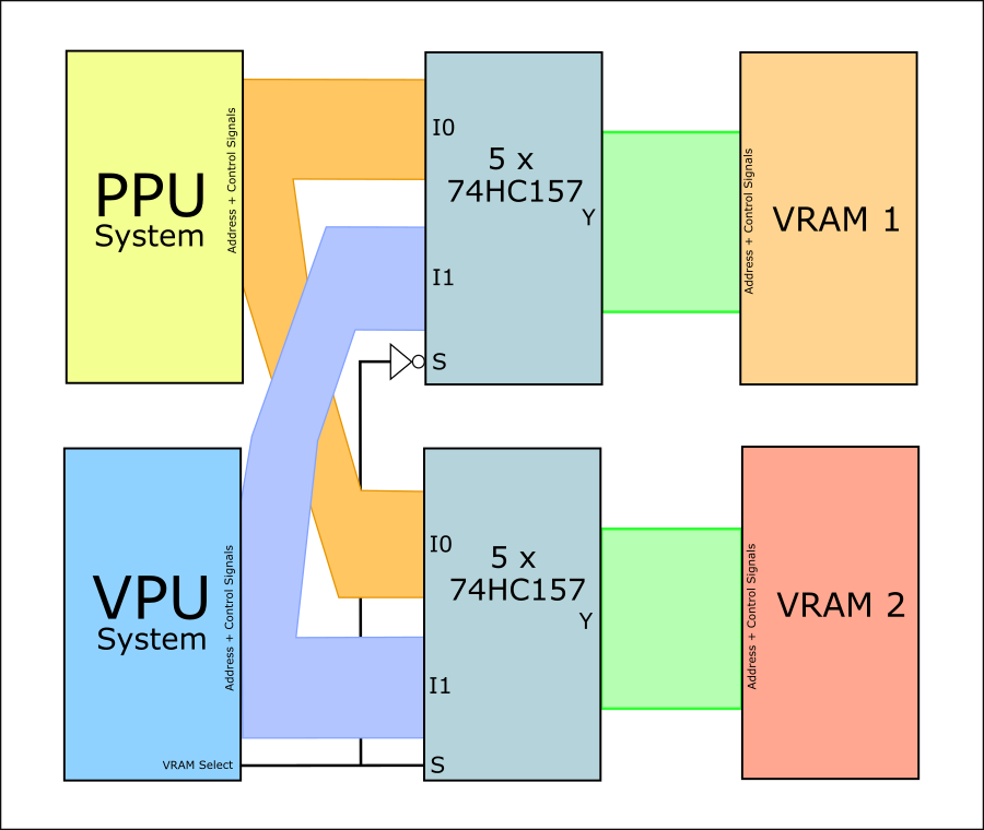
So in order to have both the VPU and PPU work simultaneously while connected to both VRAMs, meant that I needed extra components to keep the address and data buses as well as the RAM control signals separate from each component.
For this I used 74HC157 chips for the address buses as well as the control signals, this is a quad 2-input multiplexer, also known as a line data selector.
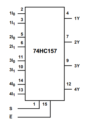
In the following diagram you can see how the 74HC157 was used with the PPU and VPU (I called them “PPU System” and “VPU System” because the signals don’t quite come from the PPU and VPU themselves as will be explained later):
For the data buses I used 74HC245 ICs:
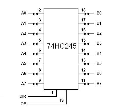
This components are bidirectional transceivers, that can allow information to pass from A to B or B to A or cut the link between the two ports.
They’re ideal to isolate the data buses of the VRAM components.
(technically I could have used these 74HC245 for the address buses and control signals also, however, it would take an extra chip, so I kept it like this).
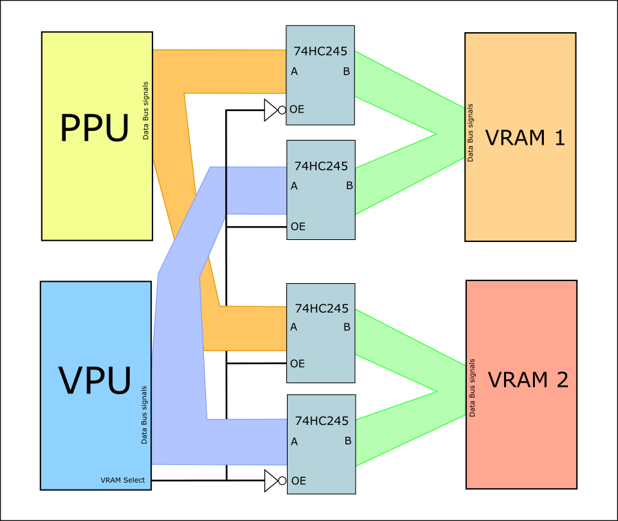
And this is how these components are layed out in the video board:
Next, I’ll go over the implementation details of the VPU and then the PPU.
VPU
The VPU does the following:
- Put the contents of the selected VRAM to screen
- Put the contents of the selected VRAM to screen for the second time (2 frames on the TV for every frame rendered)
- Change the selected VRAM
- Repeat the steps above
It ended up being an Atmega324 microcontroller (an Atmega164 would probably do fine, but I only had a 324 available).
This microcontroller outputs a TV sync signal as well as 8 bit color data, all according to PAL signal encoding.
It also interfaces with the VRAMs and decides which VRAM the VPU is connected to and which one the PPU is connected to.
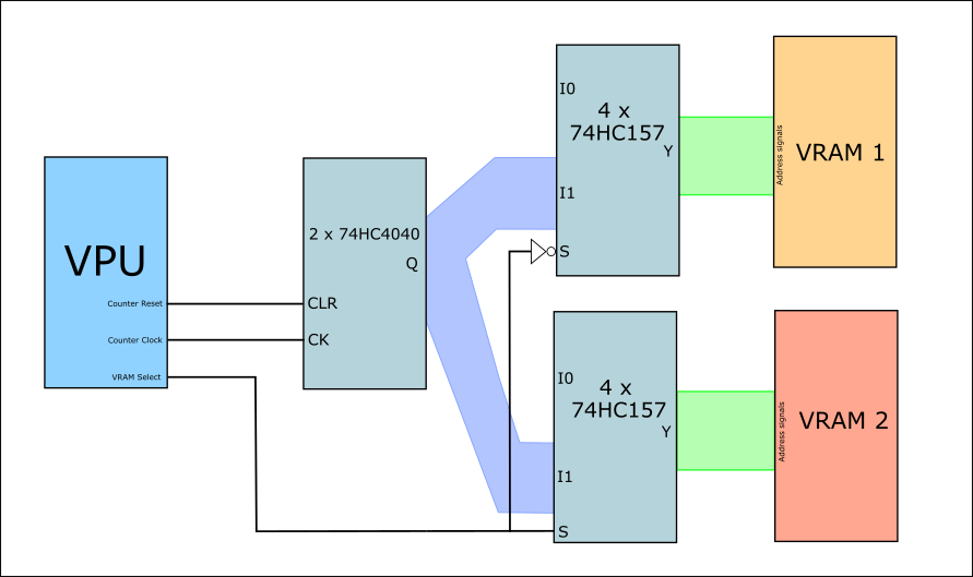
In order to shorten the time necessary to read bytes from VRAM in consecutive addresses, I added two 74 series 4040 cascade counter (74HC4040) to the project.
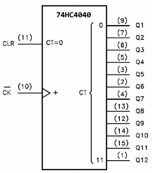
I need 16 bits to reach all the 43.008 bytes of the VRAM necessary for a frame. So I used 2 74HC4040 as each one only has 12 bits and chained them together.
By connecting the counter to the address bus of the VRAM instead of directly connecting to the microcontroller, I get to shave off a few instructions when retrieving the pixels and it also saves on the number of IO pins used for this purpose.
In the next diagram you can see a more complete picture of how the VPU is connected to VRAM.
The 4040 counters are connected to the four 74HC157s used to link the VPU and PPU to the address bus of the VRAMs.
Sending information to the screen
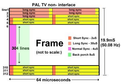
In order to send information to the screen using PAL, I need to to send a Sync signal holding the right information at the right time.
Below is a picture of the PAL timings (progressive mode and not interlaced mode, although I ended up using a hybrid mode, as progressive mode was not really 50Hz and I wanted 50Hz because it’s a good round number).
In this picture you can see exactly when and for how long the Sync signal needs to be High or Low in us (micro seconds).
Although you don’t need to get these timings exactly right to the nano-second and TVs are actually somewhat forgiving, it’s important to get them right to get a good image and, in the case of modern digital TVs, to get an image at all.
Getting the right timings in a microcontroller is usually achieved by using interrupts timed to trigger at the right time, however I used another more “naive” approach, that is calculating how long each instruction takes and coding delays in order to make sure the sync signal is set or unset at the right time.
When in a frame line the VPU also outputs color information according to the current frame being put on to screen.
In an analogue signal you can put pixels at any frequency, of course that if the frequency is too low the pixels are going to be too long or “rectangular” and the resolution in width is going to be too low (the number of pixels you can fit in a line).
To make sure I can send different color data (pixels) fast enough to the TV screen, I need to make sure the code itself doesn’t have a lot of instructions.
As I’m using an external counter (the 74HC4040 I mentioned above), I’m able to send a pixel with the following code (this code is actually a macro and not a function so I can reuse it without calling it and saving a few clocks with that):
.MACRO SetPixel
    out PORTD, READ_MEM_1_REG
    in r25, PINC
    out PORTA, r25
    out PORTD, READ_MEM_2_REG
.ENDMACRO
Like I mentioned above, the microcontroller has its 32 IO pins divided into 4 “ports” of 8 pins each (Ports A, B, C and D), and I’m able to set and read from 8 pins at a time using single “in” and “out” instructions.
For the VPU, I used Port D for the pins that control the VRAM and the counter mentioned above, this way I could set them all at once, saving extra clocks.
Port C (referred to as PINC when used as an input) is the Data bus from the current VRAM.
Port A is the color output for the TV (the 8 pins deliver RGB color, 3 pins for Red, 3 pins for Green and 2 for Blue, making up RGB 332 color space).
In the “SetPixel” code, READ_MEM_1_REG and READ_MEM_2_REG set the pins connected to the VRAM and the external counter to retrieve the current byte and add 1 to the counter. Inbetween I retrieve the color byte from VRAM and send it to the TV.
This way, by chaining 224 “SetPixel”s, I can retrieve 224 consecutive bytes from the VRAM (the pixels) and send its values as color information to the TV with just 4 instructions.
This code takes 4 clocks to execute.
And because I use 4 instructions for each pixel, the pixel clock (the frequency at which pixels are drawn, also known as dot clock) is of 5 Mhz.
This frequency is sufficient for the resolution I was going for, looking at the picture above describing the PAL timings, the visible part of screen is drawn in 52 us (micro seconds) and with a pixel being drawn every 200ns (5 Mhz), it means we can potentially draw 320 pixels (although not all of these pixels would be visible, CRT TVs usually don’t show the whole image and hide the edges).
The full code to send a visible line to the TV looks like this:
// ******** Memline *********
// Normal Sync  - 4us
// Back porch   - 8us
// Data         - 52us
Memline:
    cbi PORTB, 0    // Set Sync signal to low (2 clocks)

    //   Wait till backporch (78 clocks)
    ldi  r18, 26
LMemLine1:
    dec  r18
    brne LMemLine1

    sbi PORTB, 0    // Set Sync signal to high (2 clocks)

    // Wait till end backporch (198 clocks)
    ldi  r18, 66
LMemLine2:
    dec  r18
    brne LMemLine2

    // 224 * 4 clocks
    SetPixel10
    SetPixel10
    SetPixel10
    SetPixel10
    SetPixel10
    SetPixel10
    SetPixel10
    SetPixel10
    SetPixel10
    SetPixel10
    SetPixel10
    SetPixel10
    SetPixel10
    SetPixel10
    SetPixel10
    SetPixel10
    SetPixel10
    SetPixel10
    SetPixel10
    SetPixel10
    SetPixel10
    SetPixel10
    SetPixel
    SetPixel
    SetPixel
    SetPixel

    SetBlackPixel  // 4 clocks

    //   Wait till end of line (92 clocks)
    ldi  r18, 30
LMemLine3:
    dec  r18
    brne LMemLine3
    rjmp PC+1

    ret
Here the “well-timed code” can be seen as I have to know exactly how long each instruction takes to execute so as to time everything correctly. Luckily the AVR architecture (the CPU architecture of the microcontroller) allows me to do that as the instructions have predictable execution clocks.
All the clocks in the function add to 1272 clocks and because this is a function being called from another spot on the code we need to add 8 more clocks, 4 for the “ret” instruction and another 4 for the “call” instruction of the folowing line being sent to the TV.
This adds to 1280 clocks, which at 20 Mhz is 64.000 ns or 64 us which corresponds to the time a line should take in PAL (you can check the picure above with PAL timings).
All the code was done in AVR assembly and in this manner.
RGB encoder
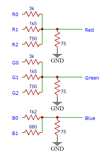
The VPU with the Sync signal, the color information (in RGB) and the help of a resistor DAC is able to generate an RGB PAL signal.
Here is diagram of the resistor DAC to convert the 8-bit color information into 3 analog signals:
However I really wanted to also have a composite signal for TVs without RGB input.
In order to achieve this I used an RGB encoder chip, a Sony CXA1645. This is a vintage chip and was used in retro consoles such as the Sega Saturn.
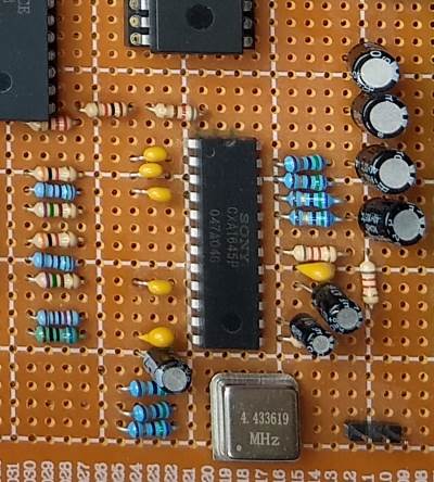
This chip is able to output RGB, composite and S-Video. I only use the RGB and composite outputs.
Output connector
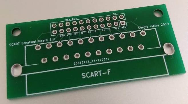
The Video (and audio) output connector of choice was a SCART connector.
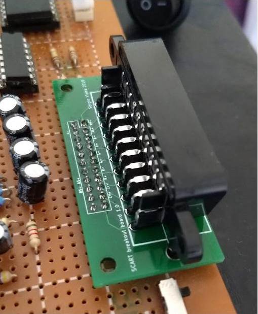
This connector was and still is quite common in my country (Portugal) and it enables me to output composite and RGB video as well as audio in one socket.
I designed and ordered a breakout board for the SCART socket as its pins didn’t fit into the protoboard.
PPU
The PPU’s firmware is the most complex in this whole project. At first it was entirely programmed in AVR assembly, now it has a few sections in C and others in assembly (it should be the other way around, I know, I should’ve started in C and moved to assembly, but oh well..).
The reason I started developing it in assembly is because from the start I knew I had to get the best performance from the code in other to push the most complexity I could into the graphics.
The PPU has the funcion of rendering the actual frames. It can use internal graphics (which are limited graphics stored in the firmware) which I call CHR-ROM or use an external RAM chip as the source of graphics: CHR-RAM.
The PPU’s operates as follows:
- Copy the contents of the PPU-RAM to internal RAM.
- Send the NMI signal to the CPU
- If the PPU Mode is CHR-ROM:
- Draw background with internal graphics
- Draw sprites with internal graphics
- If the PPU Mode is CHR-RAM:
- Draw background with CHR-RAM graphics
- Draw sprites with CHR-RAM graphics
- Draw overlay with CHR-RAM graphics
- Draw sprites over the overlay with CHR-RAM graphics
- If the PPU Mode is copy to CHR-RAM:
- Copy PPU-RAM contents to CHR-RAM
- Set the PPU Mode to Finished copying
- Wait for the VPU to signal the VRAM has switched
- Repeat
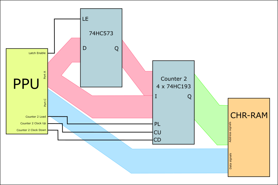
The PPU itself is connected to 3 different RAMs simultaneously and, being an Atmega1284 has only 32 IO pins, this meant that I had to figure out a way to connect everything together without losing too much performance.
Next I’m going to explain how the PPU interfaces with all these components.
Interface with the CPU
The CPU communicates with the Video system solely through the PPU-RAM.
This 4 KB RAM interfaces the CPU and the PPU.
The 8 data lines of the PPU-RAM are directly connected to one of the ports of the PPU (Port C).
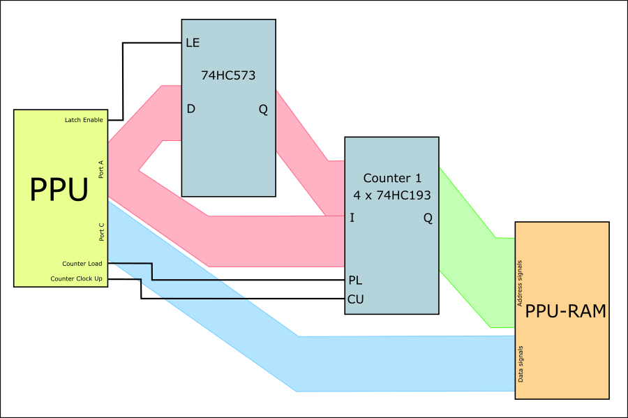
The 12 address lines are not directly connected to the microcontroller’s GPIOs, I used counter chips again, as with the VPU, this time I used 74HC193 counters, these counters have some advantages in relation to the 74HC4040 counters, they can be set with a starting value and they are bi-directional.
This way I can read specific regions of the memory without having to start from address 0, and I can read it backwards (which does not come in handy in this case).
In order to set the initial address to the counter, I use a latch (74HC573), so that I can reuse the same port of the PPU to set the whole address (Port A).
This is how the PPU and PPU-RAM are connected:
Using these counters I have the same advantages as with the VPU, I use less GPIOs and I’m able to save precious clocks, here’s some code that reads from PPU-RAM and stores in internal RAM:
    ...
	ldi r16, READ_MEM_1 // READ_MEM_1 = Clear CE and OE in the RAM, Clear Clock Up in the counter
	mov r4, r16
	ldi r16, READ_MEM_2 // READ_MEM_2 = Set CE and OE in the RAM, Set Clock Up in the counter
	mov r5, r16
	ldi r16, 0x00
	out DDRC, r16       // Set the data PORT to input
	out PORTC, r16

	SetMemPPURAM        // Select the PPU-RAM as the RAM to interact with
	SetMemClk           // Set the Counter clock to high
	ldi r16, 0
	SetAddrLatch        // Set the Latch to latch the input data
	out PORTA, r16      // Set the latched value to 0
	ClearAddrLatch      // Set the Latch to output the latched data (higher part of the address output as the initial value to the counter)
	out PORTA, r16      // Set the lower part of the address to 0 (initial value output to the counter)
	ClearMemLoad        // Set the Load pin in the counter to low, so as to store the initial value, which is 0 because of the code above)
	nop                 // delay for the counter to keep up
	SetMemLoad          // Set the Load pin to High, so as stop storing the initial value

	out PORTD, r4       // READ_MEM_1

	ldi r17, 64
GetPPURAMLoop:
	ldi r18, 64         // Loop 64 x 64 times = 4096 times
GetPPURAMLoop2:

	// Read Byte
	in r16, PINC        // Save byte from the PPU-RAM to an internal register
	out PORTD, r5       // READ_MEM_2
	nop                 // delay for the RAM and counter to keep up
	out PORTD, r4       // READ_MEM_1
	st Z+, r16          // Store the byte in the internal RAM address ZH,ZL and increment Z

	dec r18
	brne GetPPURAMLoop2
	dec r17
	brne GetPPURAMLoop
    ...
Important notes about the code above:
The SetMemPPURAM macro chooses which of the 3 RAMs I’m working with, this will be discussed further down the post.
In this code the counter is set to all zeros (16 bit), and then the bytes are read from the PPU-RAM (4096 bytes or two nested cycles of 64 each).
The nop in the part where the byte is read is due to the RAM and counter not being fast enough when using a 20Mhz microcontroller, so a nop was needed to act as a delay between interactions. The dual-port RAM used for PPU-RAM is actually an 100ns RAM, which means it works reliably at a maximum frequency of 10Mhz, so when working with a microcontroller which is twice as fast, that has to be taken into consideration.
Had I not used external counters, and the code would be more complex in the inner loop, I would have to increment the address and output two PORTs (because 8 bits are not enough) and still fetch the data and store to internal RAM, it would have been over 4 instructions.
As to the information stored in the PPU-RAM:
The 4 KB present in the PPU-RAM are then utilised by the CPU to describe the scene to be rendered in the following frame by the PPU and later put to the screen by the VPU.
The memory is mapped this way:
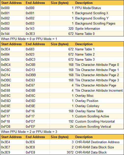
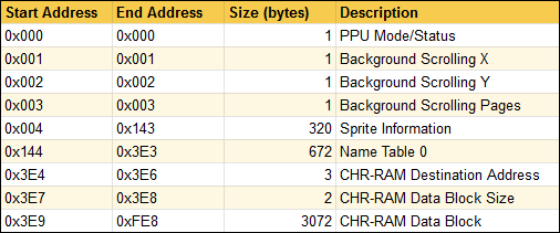
The first byte of the RAM serves as a PPU Mode/Status byte.
It switches the PPU into several modes of operation.
PPU Mode = 0:
- CHR-ROM mode (default mode). In this mode the graphical capabilities are not as extensive as in the following mode (not only because of how fast I could access the PPU’s internal ROM but also because I was lazy). In this mode the graphics used to render a scene are two predefined character pages that have been programmed into the PPU’s ROM. Games and programs are then restricted to these characters for graphics.
PPU Mode = 1:
- CHR-RAM mode. This is the PPU mode I’ve dedicated more time to. The graphical capabilities of this mode are better and the game/program can use up to 4 pages of characters for the background and 4 pages of characters for the sprites, these characters can be loaded into CHR-RAM by the CPU, making them fully customizable. When the console boots, the CHR-RAM has random information, so it’s necessary to load it first with meaningful graphics before using it.
PPU Mode = 2:
- CHR-RAM copy mode. This mode uses a different memory mapping, and serves to copy information from the CPU to the CHR-RAM, I’ll explain this in detail in a chapter ahead. In this mode a scene is also rendered in a more limited way using CHR-ROM graphics.
PPU Mode = 3:
- CHR-RAM copy mode complete. The PPU sets the PPU Mode to 3 when it’s in the PPU Mode 2 and the copy is complete. This way the CPU knows when it can use the PPU-RAM for another purpose, whether to copy more information to the CHR-RAM or to use it to draw a frame.
Interfacing with VRAM
When interfacing the PPU with the VRAM I took exactly the same approach as with the PPU-RAM and reused the same counter ICs, using the control pins of the RAM to choose when I’m using one RAM or the other.
Of course this meant I couldn’t use both of them simultaneously or even interleave the access between them easily as I had to keep changing the address of each.
This wasn’t an issue as I wasn’t planning to use them together.
The only difference in this interface is what was described above on how the VPU and PPU access alternate VRAMs, but when coding the firmware in the PPU, we can consider that the PPU is accessing the VRAM chip, although of course it is accessing one of the VRAM chips and the next frame it’ll be accessing the other one.
Here’s an example of how VRAM is accessed:
...
	SetMemVRAM      // Set memory to VRAM
	SetMemClk       // Set Clock pin in counters to high

	ldi r16, 0
	SetAddrLatch    // Set the Latch to latch the input data
	out PORTA, r16  // Set the latched value to 0
	ClearAddrLatch  // Set the Latch to output the latched data (higher part of the address output as the initial value to the counter)
	out PORTA, r16  // Set the lower part of the address to 0 (initial value output to the counter)
	ClearMemLoad    // Set the Load pin in the counter to low, so as to store the initial value, which is 0 because of the code above)
	nop             // delay for the counter to keep up
	SetMemLoad      // Set the Load pin to High, so as stop storing the initial value
...
	elpm r23, Z+    // Retrieve the color information from internal ROM (address stored in register Z)
	out PORTC, r23	// Output the retrived color information to PORT C
	out PORTD, r4   // VRAM WE pin to high, VRAM CE pin to low, Clock Up pin in counter to low.
	nop             // delay
	out PORTD, r5   // VRAM WE and CE pins to high, Clock Up pin in counter to high.
...
Interfacing with CHR-RAM
Interfacing the CHR-RAM was one of last things I did with the video board.
At this point the console was already working with internal pre-defined graphics.
However I wanted it to have custom graphics, it was an important thing for me.
It meant that every game/program could output specific graphics.
For that reason I included the CHR-RAM.
It is an 128 KB RAM, and I use it fully.
Logically it’s separated into two banks, the first 64 KB hold background graphical information and the other 64 KB hold sprite graphical information.
The way the graphics are stored in this RAM is the following.
8x8 pixel characters with 8bpp or 1 byte por pixel are stored contiguous in memory (64 bytes).
And for each 256 characters, I call it a “character page”.
Therefore, the CHR-RAM has 4 character pages for background graphics and 4 character pages for sprite graphics.
In terms of how this component needed to be connected to the PPU, it had to be done differently.
First off I needed to access CHR-RAM at the same time or almost at the same time as VRAM. So I need another set of counters to act independently from the one manipulating the VRAM adress:
Another thing that would be important was to make this counter count backwards as well, for flipped sprites that I’ll talk about later.
This still doesn’t solve everything, let’s say we’re drawing the background and we need to:
- Enable CHR-RAM
- Read the color byte from CHR-RAM
- Enable VRAM
- Write the color byte to VRAM
Just the reading and writing operations takes about 4 instructions or 4 clocks, so it would take about 8 clocks everytime I need to write a pixel and there goes my performance down the drain.
I needed a way to speed it up, so I thought, since both the CHR-RAM and VRAM share the same data bus, maybe I could make the CHR-RAM read a byte and write it directly into VRAM, sort of like a DMA.
This couldn’t be done without the PPU’s assistance because in the case of drawing sprites, the PPU would still need to check if the color byte matched the sprite’s colorkey in order to draw it or not in VRAM.
In order to achieve this I couldn’t use the same control signals for both RAMS (CE, CE2, WE and OE), I used a second PLD in the project and as inputs I used the control signals as well as two other SM1 and SM2, that equate to a 2 bit Select Memory signal.
These Select Memory sinal works as such:
- SM = 0: Select VRAM
- SM = 1: Select PPU-RAM
- SM = 2: Select CHR-RAM
- SM = 3: Select Read CHR-RAM / Write VRAM Mode
The PLD returns as outputs the same inputs for the VRAM and CHR-RAM when in Select Memory 0, 1 and 2. But when in Select Memory 3, it enables me to enable both RAMS while sending read signals to the CHR-RAM and at the same time sending write signals to the VRAM.
This is how transfering information from the CHR-RAM to the VRAM looks like:
...
    SetCHRRAMBank0  // Set the CHR-RAM lower 64KB (Bank 0), Tile characters

    SetMem2Clk      // Set Counter 2 Clock to high
    SetMemClk       // Set Counter 1 Clock to high

    // Set the Counter 1 value (VRAM address)
    ldi r16, 0
    SetAddrLatch
    out PORTA, r16
    ClearAddrLatch
    out PORTA, r16
    ClearMemLoad
    nop
    SetMemLoad

    SetMemCHRRAMVRAM    // Set Selected Memory to 3
...
    // Setting the Counter 2 value (CHR-RAM address)
    SetAddrLatch
    out PORTA, ZH
    ClearAddrLatch
    out PORTA, ZL
    ClearMem2Load
    nop
    SetMem2Load
...
    ldi r16, READ_WRITE_MEM_1
    mov r4, r16
    ldi r16, READ_WRITE_MEM_2
    mov r5, r16
    ldi r16, READ_WRITE_MEM_3
...
    // Transfering byte from CHR-RAM to VRAM
    out PORTD, r4   // CHR-RAM CE to low VRAM CE and both WE to high, Clock Counters 1 and 2 to low
    out PORTD, r5   // VRAM CE to low, VRAM WE to low
    nop
    out PORTD, r6   // CHR-RAM CE and VRAM CE to high, Clock Counters 1 and 2 to high
...
And transfering information from CHR-RAM to the VRAM while testing it for the colorkey (used in sprites):
...
DrawSpriteCHRRAMLineLoop:
	out PORTD, r4   // CHR-RAM CE to low VRAM CE and both WE to high, Clock Counters 1 and 2 to low
	nop             // Delay to guarantee the byte is the data bus
	in r23, PINC    // Retrieve the byte being transfered
	cp r23, r20     // Compare if it's the same as the colorkey
	breq PC+2

	out PORTD, r5   // VRAM CE to low, VRAM WE to low
	out PORTD, r6   // CHR-RAM CE and VRAM CE to high, Clock Counters 1 and 2 to high

	dec r24
	brne DrawSpriteCHRRAMLineLoop
...
Moving information from the CPU to the CHR-RAM
For the custom graphics to be loaded into the CHR-RAM, this RAM needs to be accessed by the CPU.
Originally I intended for the CPU to have direct access to the CHR-RAM together with the PPU, however when it came to actually figuring out how to put the CHR-RAM into the project, I felt that in order to do this I had to add too many more components and I felt the project was already too complex.
So I went with another approach, which was to have the PPU as an intermediary, carrying information from the CPU and putting it into the CHR-RAM.
In consoles such as the Sega Mega Drive (Genesis in the US), for example, the CPU has to activate a DMA to transfer bytes to the Video RAM, what I did is similar, if not a bit more crude.
The CPU can then copy information from the SD Card, for example, to the PPU-RAM, 3 KB at a time, because PPU-RAM has only 4KB in total, and set the PPU Mode in the PPU-RAM to “Copy to CHR-RAM”.
If the PPU Mode is “Copy to CHR-RAM”, this means that the PPU-RAM has this mapping:
While in PPU Mode 2 or 3, a scene is also rendered using only one nametable and sprites (these graphical components will be explained below).
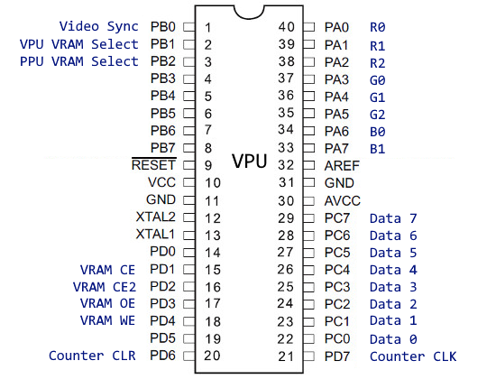
PPU Signals
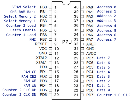
Here are the input/output signals connected to the PPU (an Atmega1284):
Component Layout
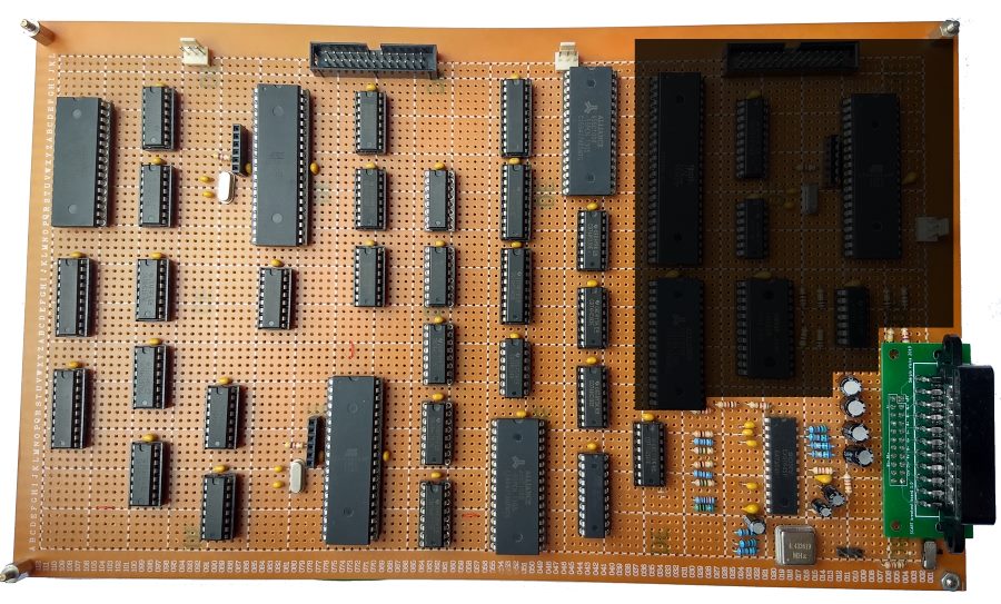
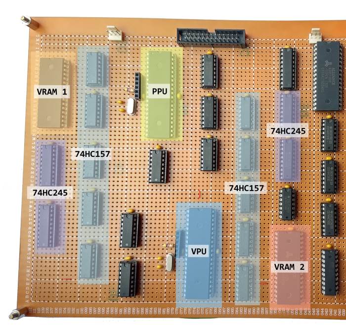
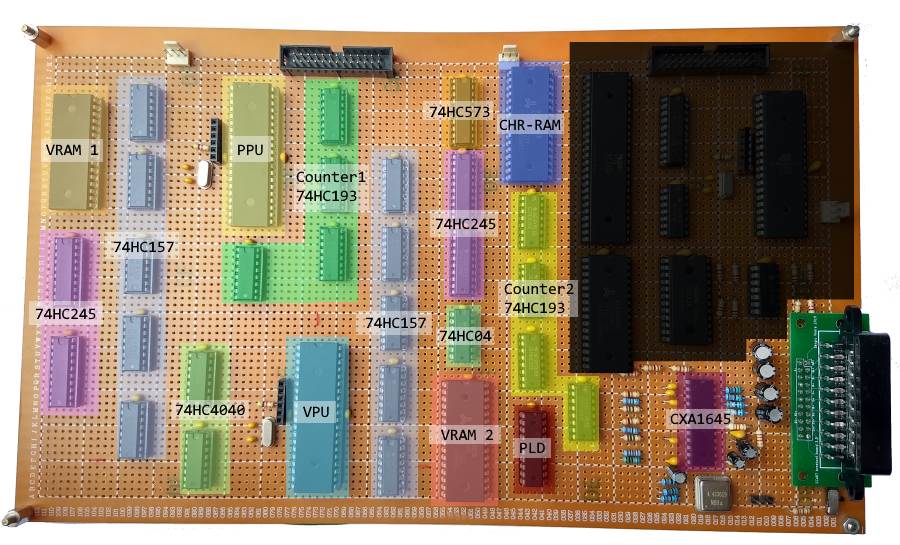
This is the layout of the components described above in the video board:
Graphical capabilities
With the implementation described above these are the graphical capabilities I was able to put into the console:
A frame can be rendered using internal graphics or custom graphics residing in the CHR-RAM. This is set through the PPU Mode as described above.
Graphics are composed of 8x8 pixel characters, so all elements are rendered using this “building blocks”.
Each character can have a total of 256 colors in RGB332 space (3 bits for red, 3 bits for green and 2 bits for blue):

When using internal graphics the program is limited to 256 predefined characters for the background and 256 predefined characters for sprites (1 character page for background and 1 for sprites). In this mode the graphical capabilities are more modest:
-
One scrollable background layer.
-
64 Sprites restricted to the size of 8x8.
When using custom graphics (CHRRAM), a scene can be composed of the following:
-
One Background layer
-
64 Sprites
-
Horizontal Overlay Stripe composed of 28x6 characters
Also when using CHR-RAM, a program can use 4 pages of characters for background and 4 character pages for sprites.
Each character page holds 256 characters.

The next sections detail each of these components.
Background
The frame has 224x192 pixels and because each character has 8x8 pixels, this equates to 28x24 characters.
To have the possibility for a larger “virtual” background that can be scrolled, there are four nametables (also known as tilemaps or pages, I’m not good with names…).
A nametable is an array that stores which character is where in the background.
Each one of these nametables has the same size as the size of the frame and are a map of 28x24 characters. The 4 of them are contiguous to each other in this configuration:
To control how these 4 nametables are rendered as the background there are 3 bytes:
- Scroll X
- Scroll Y
- Scroll Pages
The Scroll Pages determines which nametable is on the left and on top. Only the least significant bits are taken into consideration.
If the bit 0 is set to 0, the nametable to the left is 0 or 2 (depending on the vertical scroll position) if it’s set to 1, the nametable is 1 or 3.
If the bit 1 is set to 0, the nametable on top is 0 or 1 (depending on the horizontal scroll position) if it’s set to 1, the nametable is 2 or 3.
The Scroll X determines how much of an horizontal scroll there is on the nametables that are rendered to the left. It must have a value between 0 and 223.
The Scroll Y byte determines how much of a vertical scroll there is on the nametables that are rendered on top. It must have a value between 0 and 191.
Attribute Tables
There is also the possibility to give an attribute from 0 to 3 to each of the tiles/characters in every nametable.

And it’s possible to define on which of the 4 character pages each attribute is getting the graphics from and add an increment to tiles that have certain attributes.

To make this possible there is an area in the PPU-RAM with four attribute-tables, each table has 168 bytes, each byte corresponds to 4 tiles of the corresponding nametable.
The 2 least significant bits is the attribute of the first tile, the next 2 bits is the attribute of the second tile, etc.
(Check out the PPU Simulator to better understand how attribute tables work and how they’re organised)
Custom Scrolling
Apart from the scrolling of the four nametables described before, I’ve also added the possibility of scrolling the background starting in predetermined vertical lines.
It’s possible to have different horizontal scroll positions in 64 distinct lines and different vertical scroll positions in 8 distinct lines.
In the PPU-RAM, position 0xF17 is the byte that can be set to 1 to activate Custom Scrolling.
Next to this byte is the region to set custom horizontol scrolling composed of 64 x 3 bytes.
And next to this one is the region for custom vertical scrolling composed of 8 x 3 bytes.
The 3 bytes that define the scroll are the following:
- The line from which the scroll will start
- The value of the scroll
- The starting nametable (page) for the scroll (only least-significant bit used)
When custom scrolling is active, the way this works is:
- The PPU sets the scroll to the background scrolling
- The PPU reads the first 3 bytes of custom horizontal scroll
- It compares the current line being drawn to the first byte, if it is the same it sets the horizontal scrolling to the two other bytes and reads the next 3 bytes
- The PPU reads the first 3 bytes of custom vertical scroll
- It compares the current line being drawn to the first byte, if it is the same it sets the vertical scrolling to the two other bytes and reads the next 3 bytes
- As it renders all the lines, line by line it does the same comparisons for each line
Custom-scrolling enables effects such as parallax and split-screen.

Sprites
Objects on top of a background that can move pixel by pixel independently of said background are essential components of a 2D game.
For this reason, this video game console is able to render 64 moving objects (also known as sprites).
Each of the sprites has the following configurable properties:
-
Horizontal Position (32 being on the left edge of the frame)
-
Vertical Position (32 being the top of the frame)
-
Character Page: What of the 4 character pages the sprite character is located.
-
Character: Which of the 256 sprites in the selected character page.
-
Colorkey: The color that is not drawn.
-
Horizontal Flip: If the sprite should be drawn flipped horizontally.
-
Vertical Flip: If the sprite should be drawn flipped vertically.
-
Width 8 or 16 pixels: The width of the sprite having 8 or 16 pixels.
-
Height 8 or 16 pixels: The height of the sprite having 8 or 16 pixels.
-
Above or below overlay: If the sprite should be above or below the overlay.
The properties for each sprite are represented in PPU-RAM by 5 bytes. And the information for the 64 sprites are contiguous in memory starting at address 0x004 filling 320 bytes.
The 5 bytes of each sprite represent the following:
- Misc attributes:
- Bit 0: Active/Visible
- Bit 1 and 2: Character Page
- Bit 3: Flip horizontally
- Bit 4: Flip vertically
- Bit 5: Above overlay
- Bit 6: 16 pixels of width (if unset the width is 8 pixels)
- Bit 7: 16 pixels of height (if unset the height is 8 pixels)
- Character
- ColorKey
- Horizontal Position
- Vertical Position
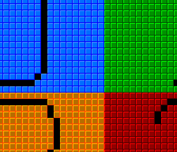
When a sprite has a width and/or height bigger of 16 pixels, it’s going to use more than one character.
So in these cases the sprite will be drawn using adjacent characters to the one configured for it.
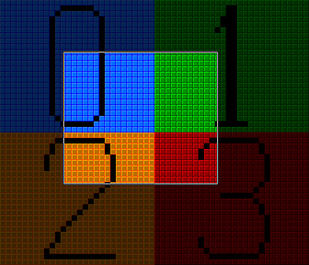
![]()
For objects bigger than 16x16 pixels, we can simply combine several sprites and move them together to get a bigger object.
![]()
Overlay
The last graphical component is an overlay.
I took this idea from observing the Uzebox project and I found this to be an interesting solution to HUDs in games, for example.
So, it’s possible to place a 28x6 tiles horizontal strip on top of the background and sprites.
This strip can be composed of background characters or of sprite characters, in which case it has transparency.
The strip can also be positioned anywhere vertically.

Simulator
In order to better understand how the PPU renders a screen and the interaction between the CPU and the PPU, I’ve made an online PPU simulator.
Here you can change the PPU-RAM and see the effects in real-time and even automate the changes every frame (in essence simulating a CPU).
Or you can just run the example scripts.
Check out the PPU Simulator here.
And this is it
I’ve had a few requests to write about how the video was handled in this project and so I tried to be as extensive as I could.
It took a lot of time to compile all the information, get the pictures, draw the diagrams, etc.
There was so much to talk about. It might be too much information for some and not enough for others.
I hope this helps someone with his or her projects.
And if you’ve reached this far, thank you for reading it. :)
As always, any question or suggestion please comment below or reach me in my twitter account @IntRegister